
PICT 2026 - Lecture 02: STM32F4xx Internals
Workshop Series, PICT, Pune, 2026
STM32F4xx Internals
Materials
📊 Slides
🎥 Video Recording
Lecture 2 – STM32F40xx Architecture and Clock / Bus Systems
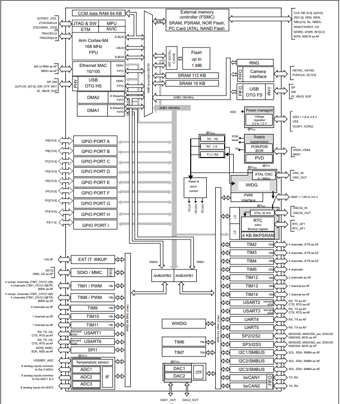
Right. We have now understood the basics of a Cortex M-4 MCU. Now, we shall take a look at the actual implementation of the Cortex M-4 architecture onto an MCU, which you now hold in your hands. Here is what the product specification from ST itself says about the F407 MCU -
The STM32F407/417 lines are designed for medical, industrial and consumer applications where the high level of integration and performance, embedded memories and rich peripheral set inside packages as small as 10 x 10 mm are required. The STM32F407/417 offers the performance of the Cortex™-M4 core (with floating point unit) running at 168 MHz.
Performance: At 168 MHz, the STM32F407/417 deliver 210 DMIPS/566 CoreMark performance executing from Flash memory, with 0-wait states using ST’s ART (Adaptive Real-Time) Accelerator. The DSP instructions and the floating point unit enlarge the range of addressable applications.
Power efficiency: ST’s 90 nm process, ART Accelerator and the dynamic power scaling enables the current consumption in run mode and executing from Flash memory to be as low as 238 µA/MHz at 168 MHz.
Rich connectivity: Superior and innovative peripherals - Compared to the STM32F4x5 series, the STM32F407/417 product lines feature Ethernet MAC10/100 with IEEE 1588 v2 support and a 8- to 14-bit parallel camera interface to connect a CMOS camera sensor.
2x USB OTG (one with High Speed support).
Audio: dedicated audio PLL and 2 full duplex I²S
Up to 15 communication interfaces (including 6x USARTs running at up to 11.25 Mbit/s, 3x SPI running at up to 45 Mbit/s, 3x I²C, 2x CAN, SDIO) Analog: two 12-bit DACs, three 12-bit ADCs reaching 2.4 MSPS or 7.2 MSPS in interleaved mode
Up to 17 timers: 16- and 32-bit running at up to 168 MHz
Easily extendable memory range using the flexible static memory controller supporting Compact Flash, SRAM, PSRAM, NOR and NAND memories Analog true random number generator
The STM32F417 also integrates a crypto/hash processor providing hardware acceleration for AES 128, 192, 256, Triple DES, and hash (MD5, SHA-1).
Integration: The STM32F417x portfolio provides from 512 Kbytes (on WLCSP90 package only) to 1 Mbyte of Flash, 192 Kbytes of SRAM and from 64 to 144 pins in packages as small as 4 x 4.2 mm.
The STM32F407/417 product lines provide from 512 Kbytes to 1 MByte of Flash, 192 Kbytes of SRAM, and from 100 to 176 pins in packages as small as 10 x 10 mm.
Well, the info dump is cool and all, sounds like it’s a superlative processor after all. But we are here to find out about what does it all mean, aren’t we? What are the actual uses of these impressive sounding peripherals and how do they exactly work? Well, I sure am glad that you asked!
This lecture shall go deep into a few of these peripherals, and to tie it all together, we shall take a look at the Clock and Bus interfaces of this processor, which helps us understand how do these peripherals get their juice (power) and how do they communicate their data to and from the central CPU.
MCU Memory and Access
Flash
For any sort of compute system to function, a fundamental requirement would be a space to function within. A space to store and retrieve things as and when demanded by an operation. The Flash memory, is that playground for our MCU.
If we talk specs, there is a flash memory of 512 Kbytes or 1 Mbytes available for storing programs and data, plus 512 bytes of OTP memory. But what does it mean? And how does a processor interact with it?
Like I mentioned, the flash memory acts as the playground for any and all operations that the MCU wished to do. It serves as non-volatile storage for program code and constant data, allowing the MCU to retain its instructions and essential information even when power is removed. It is used to store the firmware or application code that the MCU executes upon startup, and it supports in-circuit programming, enabling updates without removing the chip from the circuit.
In terms of our own board, there’s provisions for Byte, half-word, word and double word write on the flash, along with sector and mass erase capabilities. The flash memory is organized as follows: – A main memory block divided into 4 sectors of 16 Kbytes, 1 sector of 64 Kbytes, 7 sectors of 128 Kbytes – System memory from which the device boots in System memory boot mode – 512 OTP (one-time programmable) bytes for user data The OTP area contains 16 additional bytes used to lock the corresponding OTP data block. – Option bytes to configure read and write protection, BOR level, watchdog software/hardware and reset when the device is in Standby or Stop mode.
Now, how the hell do we interact with this? Simple - via buses! A bus, is nothing but a collection of wires that transmit signals. Multiple wires are bundled together, which helps transmit a big chunk of data at the same time - a.k.a a parallel interface. When it comes to the Flash, there’s 2 buses, the I-code and the D-code bus.
The I-Code bus stands for the Instruction-Code Bus, while the D-Code bus means Data Bus. The Cortex M-4 arch is Harvard in nature, which means it had 2 separate buses for an Instruction and a piece of Data. Since the instructions are to be fetched in a linear manner and data fetches are irregular in nature, it makes sense to separate these two in order to not interrupt the flow of instructions with data stalls!
ART accelerator (prefetch, cache, wait states) Basically, the ART accelerator helps speed up the instruction fetch access of the Cotred-M4 processor’s internal memory. Basically, a part of code is stored into a segment of memory that helps provide near-instant access to the CPU, thus avoiding latency due to memory wait states.
The cache memory is organized in 64 lines of 256 bits each. Each line contains eight 32-bit segments. Each segment can contain one 32-bit or two 16-bit instruction codes. The cache buffer is an extra line of 256 bits keeping a copy of one of the cache lines. For a cacheable access, it allows the instruction fetch from cache in case of a cache hit and it manages the cache memory line refill (instruction code load) in case of a cache miss. For non-cacheable memory accesses, the instruction is directly fetched from memory.
SRAM
- Main SRAM This, is the volatile memory of the MCU. This is the place where all the run-time compute is performed at. All the local variables, function call return addresses, CPU registers and system context during switching is stored at. The MCU has 192KB of System SRAM and 4KB of backup SRAM. The embedded SRAM can be accessed as bytes, half-words (16 bits) or full words (32 bits). Read and write operations are performed at CPU speed with 0 wait state. It is quite fast in it’s speed, with the obvious downside of it being volatile in nature.
- CCM SRAM (Core-Coupled Memory) This is a special memory that guaranteed 0 wait-state access during the runtime, due to it having a dedicated bus to the MCU’s core. We can explicitly store data into the CCM by writing to specific addresses. It is often used to store compute data for real time control loops and look-up tables for processing critical data.
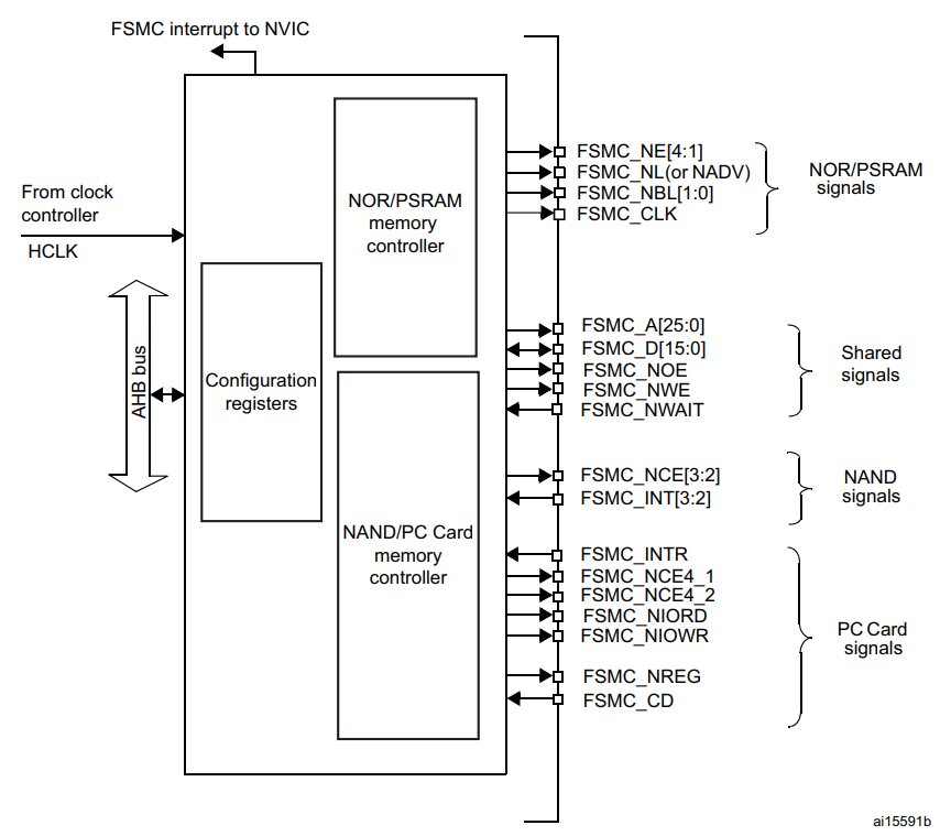
FSMC (Flexible Static Memory Controller)
Quite often, it just so happens that the on-chip memory does not fulfill the requirements of the system that is being developed. Afterall, we are talking about KILOBYTES of RAM here, y’all! Interfacing an external chip of memory with the MCU is quite common, and dare I say the norm these days in the industry. ST recognizes this and decided to develop a dedicated interface for interacting with external memory chips, called the FSMC.
This block is used to provide an interface with (a)synchronous memories and 16-bit PC memory cards. It translates the AHB instructions to the appropriate external memory protocol, while keeping the timing requirements of the device. All external memories share the addresses, data and control signals with the controller. Each external device is accessed by means of a unique chip select. The FSMC performs only one access at a time to an external device.
DMA
Direct Memory Access (DMA) is used to provide high-speed data transfer between peripherals and memory, as well as between memory locations. DMA allows data movement without continuous CPU intervention, freeing CPU resources for other tasks and reducing overall system latency.
The STM32F407 includes two DMA controllers, DMA1 and DMA2, providing a total of 16 streams, with 8 streams per controller. Each stream can be mapped to one of up to eight channels, where each channel corresponds to a specific peripheral request. Arbitration logic within the DMA controller handles priority when multiple DMA requests occur simultaneously.
The DMA controllers connect to the system through AHB master interfaces, allowing access to both memory and peripherals. Data transfers can be configured as 8-bit, 16-bit, or 32-bit accesses, depending on peripheral requirements and memory alignment. Each DMA stream includes an optional FIFO buffer that improves bus efficiency and supports burst transfers. The FIFO threshold level can be configured in software to 1/4, 1/2, or 3/4 of its total capacity.
When operating in direct mode (FIFO disabled), the DMA uses a single internal data buffer to minimize latency. In memory-to-peripheral transfers, this allows one data item to be preloaded so that the transfer can occur immediately when the peripheral issues a DMA request. Each DMA stream can be configured for peripheral-to-memory, memory-to-peripheral, or memory-to-memory transfers, with software-programmable priorities.
DMA Transaction
Each DMA transaction has 3 operations: • A loading from the peripheral data register or a location in memory, addressed through the DMA_SxPAR or DMA_SxM0AR register • A storage of the data loaded to the peripheral data register or a location in memory addressed through the DMA_SxPAR or DMA_SxM0AR register • A post-decrement of the DMA_SxNDTR register, which contains the number of transactions that still have to be performed
After an event, the peripheral sends a request signal to the DMA controller. The DMA controller serves the request depending on the channel priorities. As soon as the DMA controller accesses the peripheral, an Acknowledge signal is sent to the peripheral by the DMA controller. The peripheral releases its request as soon as it gets the Acknowledge signal from the DMA controller. Once the request has been deasserted by the peripheral, the DMA controller releases the Acknowledge signal. If there are more requests, the peripheral can initiate the next transaction
GPIOs and Interrupts
GPIOs
In the world of Microelectronics, GPIOs act as the intermediary of all interactions between the raw, untamed power of the processor and the outer world. Pick up any microcontroller, and you’ll find these arranged in a neat array, usually along the edge of the development board (usually referred to as board GPIO ); while they are situated at the underbelly of any microprocessor, which is the side that you’d slot it along into a motherboard (Also called as the Integrated Circuit GPIOs) .
Now, on its own, the processor is of absolutely no use whatsoever in the absence of its intermediary, as it cannot either receive or send data to its environment. The GPIOs, are of no pre-defined function. It is entirely up to the user to set their function and control its behavior. As the name suggests, there are 2 primary functions that can be assigned to these pins.
When in Input mode, it is capable of receiving data from the external world. This means that the pin is programmed to be capable of receiving voltage from external Input devices, which can be anything such as your mouse, your touchscreen, or any kind of sensor such as ultrasonic, IR, and many more.
Meanwhile, when configured in its output mode, it is capable of delivering voltage signals to external devices, It may be a control signal or a feedback signal, depending on the application loop, as specified in the program written by the programmer.
Adding another level of control to the functionality of these pins is the ability to select the type of I/O (Input / Output) signal that we wish to either receive or send over any particular pin. As of today, most of the signals involved in electronics are either digital or analogue signals. A digital signal is discreet in nature, usually switching between 2 set voltage levels to represent a logical 0 and a logical 1. The analogue signals, however, are continuous in nature, with their values oscillating between 2 limiting voltage levels, usually in a periodic manner.
These pins have an upper limit, which is the maximum voltage that they can either receive or send. These are called logic levels and are usually set at either 5 volts or 3.3 volts. It is advised to adhere to these limits, as overvoltage at these pins can cause significant damage to them, rendering the pin useless.
Now, there is a special feature about these, and that is the ability of some GPIO pins to act as multi-functional pins. The thing is, not all pins of an MCU are assigned/mapped to a particular GPIO pin. The reason being there’s simply not enough space for them all to live together on a single board. This leads to a select few pins having the ability to have Alternate Functions. These functions are configurable by the user, as in, the user can decide which functionality should the GPIO Pin be configured into.
Timers and Counters
A timer (sometimes referred to as a counter) is a special piece of hardware inside many microcontrollers. Their function is simple: they count (up or down, depending on the configuration–we’ll assume up for now). For example, an 8-bit timer will count from 0 to 255. Most timers will “roll over” once they reach their max value. So, our 8-bit timer would start over again from 0 once it reaches 255.
You can apply a variety of settings to most timers to change the way they function. These settings are usually applied via other special function registers inside the microcontroller. For example, instead of counting to a maximum of 255, you might tell the timer that you want it to roll over at 100 instead. Additionally, you can often connect other hardware or peripherals inside the microcontroller to the timer, like toggling a specific pin automatically when the timer rolls over.
Here are some of the common hardware functions you’ll see with timers:
Output compare (OC): toggle a pin when a timer reaches a certain value
Input capture (IC): measure the number of counts of a timer between events on a pin
Pulse width modulation (PWM): toggle a pin when a timer reaches a certain value and on rollover. By adjusting the on versus off time (duty cycle), you can effectively control the amount of electrical power going to another device.
Interrupt & Debug Infrastructure
These are a few special signals that are given priority of being processed regardless of what is already being processed by the MCU when they are received.
Interrupts are quite curious, since they allow us to have a say over which signal gets processed on a priority. This is quite powerful when it comes to designing systems, where signals of high importance to the system’s stability - for example, the break signal in a bike or a car is supposed to be given a higher priority for being processed, over, say, the indicator being blinked?
Now, the cool thing about ST MCUs is that it has a dedicated hardware block called the Nested Vector Interrupt Controller, which takes care of managing the actual interrupt delivery of the signals that it receives. This block is responsible for managing how interrupts are accepted, prioritized, and serviced by the CPU.
Depending on the device family, the NVIC can handle 82 to 91 maskable interrupt channels, basically, reasons to interrupt the processor (apart from the 16 core Cortex-M system exceptions). Each interrupt can be assigned one of 16 programmable priority levels (4-bit priority field), allowing fine-grained control over which events preempt others. The hardware is designed for very low-latency exception handling, so critical signals are serviced almost immediately. It also integrates power-management control hooks (like sleep/wake behavior) and exposes system control registers that let firmware configure, enable, disable, or nest interrupts safely and efficiently.
In short, instead of software constantly polling for events, the NVIC lets the hardware intelligently decide who deserves the CPU first - making real-time behavior both predictable and fast.
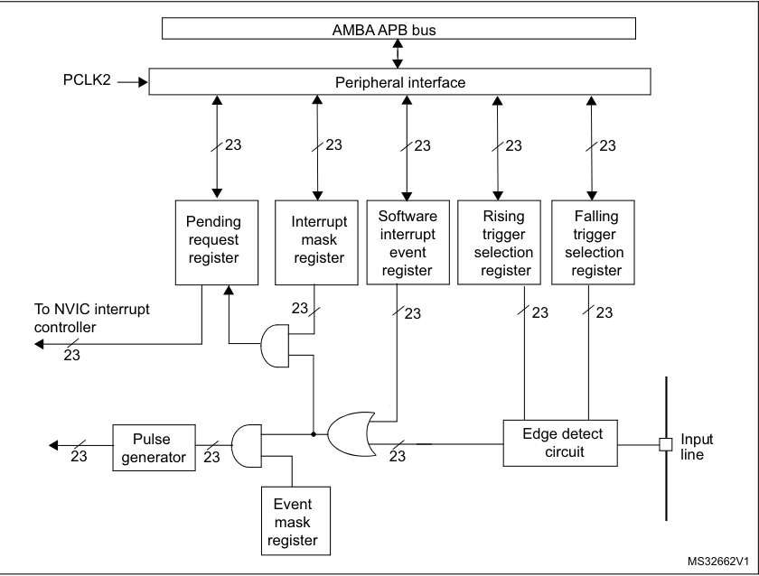
Now, who does end up providing the interrupt signals to the NVIC? Is it the external signal itself that ends up so close to the processor? Nope. It is another hardware block, called the EXTI. The EXTI block, receives the external signal and detects the edges or the signal levels. Depending on how has the interrupting signal been configured in the EXTI registers, it will turn them into interrupt requests or events.
Think about it this way - the EXTI determines if any particular signal should have the ability to generate an interrupt. The NVIC decides which interrupt gets services in case there are multiple present. The EXTI has lines, while the NVIC has channels. Depending on the board and the manufacturer, different lines may map to different channels.
You may think why the hell do we need all this hardware in the first place? Well, the answer is that interrupts need to be filtered; there’s a need to determine if the interrupt is supposed to be masked or not, which edge should be considered as the trigger for the interrupt, and a lot more. We cannot waste CPU cycles to do all this. The name of the game is to reduce the workload on the CPU, and if hardware is needed to do that, then so be it!
How Do We Tie ’Em All Together?
Clocks for Power and Buses for Memory
Clocks
 In simple words, these are power sources for the microcontroller. They are what fuels the whole operation. But why are they called clocks in the first place? Because like how clocks control everything that we do in our days, these signals are the controllers for literally everything that the MCU does. More importantly, WHEN the MCU does something, and how quickly does it get done.
Think of it as the band of a march-past. The company moves as fast or slow as the beat of the drum, right? That’s how the clocks work. They are usually crustal oscillators, which use the principal of piezoelectricity. When an electric voltage is applied to the crystal, it mechanically vibrates at a precise, natural resonant frequency determined by its physical size, shape, and cut. These vibrations generate a small electrical signal, which is amplified by an electronic circuit. The amplified signal is then fed back to the crystal, sustaining continuous oscillations. This positive feedback loop ensures the system oscillates only at the crystal’s resonant frequency, producing a highly stable and accurate electrical signal.
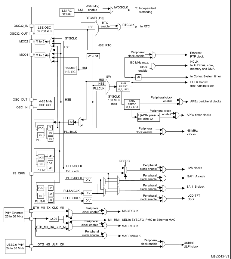
Now, there’s MULTIPLE sources for the clock signal to reach the MCU’s circuitry. Let’s take a look at them all -
HSE
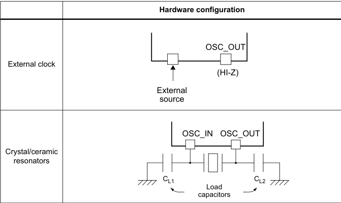 The high speed external clock signal (HSE) can be generated from two possible clock sources: •HSE external crystal/ceramic resonator •HSE external user clock The resonator and the load capacitors have to be placed as close as possible to the oscillator pins in order to minimize output distortion and startup stabilization time. The loading capacitance values must be adjusted according to the selected oscillator.
The HSE External Clock, can be a signal (square, sinus or triangle) with ~50% duty cycle has to drive the OSC_IN pin while the OSC_OUT pin should be left HI-Z. While the HSE Crystal/Ceramic Resonator has the advantage of producing a very accurate rate on the main clock. The associated hardware configuration is shown in the above picture.
HSI
The HSI clock signal is generated from an internal 16 MHz RC oscillator and can be used directly as a system clock, or used as PLL input. The HSI RC oscillator has the advantage of providing a clock source at low cost (no external components). It also has a faster startup time than the HSE crystal oscillator however, even with calibration the frequency is less accurate than an external crystal oscillator or ceramic resonator. 
LSE
This, is generated from a 32.768 kHz low-speed external crystal or ceramic resonator. It has the advantage of providing a low-power but highly accurate clock source to the real-time clock peripheral (RTC) for clock/calendar or other timing functions. The LSE Clock can remain enabled in all low-power modes and in VBAT mode because it belongs to the RTC power domain.
LSI
Finally, the is a low-speed internal RC oscillator that can be used as a low-power clock source for some peripherals, such as the independent watchdog (IWDG) and the auto-wakeup unit (AWU). The LSI Clock frequency is 32.78 kHz. The LSI Clock can be kept running when the system is in stop or standby mode, but it is not functional in shutdown or VBAT mode. It is not very accurate and cannot be calibrated.
PLL
 Think of this as the shot of espresso that we have. It boosts the clock signal from one of these sources at a max of 180 MHz when it comes to the Cortex M-4 MCUs. A phase locked loop, PLL, is basically of form of servo loop. Although a PLL performs its actions on a radio frequency signal, all the basic criteria for loop stability and other parameters are the same. In this way the same theory can be applied to a phase locked loop as is applied to servo loops.
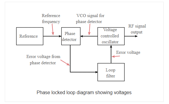
In the basic PLL, reference signal and the signal from the voltage controlled oscillator are connected to the two input ports of the phase detector. The output from the phase detector is passed to the loop filter and then filtered signal is applied to the voltage controlled oscillator. The Voltage Controlled Oscillator, VCO, within the PLL produces a signal which enters the phase detector. Here the phase of the signals from the VCO and the incoming reference signal are compared and a resulting difference or error voltage is produced. This corresponds to the phase difference between the two signals.
The error signal from the phase detector passes through a low pass filter which governs many of the properties of the loop and removes any high frequency elements on the signal. Once through the filter the error signal is applied to the control terminal of the VCO as its tuning voltage. The sense of any change in this voltage is such that it tries to reduce the phase difference and hence the frequency between the two signals. Initially the loop will be out of lock, and the error voltage will pull the frequency of the VCO towards that of the reference, until it cannot reduce the error any further and the loop is locked.
When the PLL, phase locked loop, is in lock a steady state error voltage is produced. By using an amplifier between the phase detector and the VCO, the actual error between the signals can be reduced to very small levels. However some voltage must always be present at the control terminal of the VCO as this is what puts onto the correct frequency.
The fact that a steady error voltage is present means that the phase difference between the reference signal and the VCO is not changing. As the phase between these two signals is not changing means that the two signals are on exactly the same frequency. 
Clock Tree & Prescalers
Once a clock source is selected and optionally multiplied using the PLL, the resulting system clock cannot be fed directly to every part of the MCU at the same rate. Different blocks inside the microcontroller have very different speed, power, and timing requirements. This is where the clock tree comes into play. The clock tree is a hierarchical distribution network that takes the system clock and divides it into multiple derived clocks, each tailored for a specific domain inside the MCU.
Prescalers sit at key junctions in this clock tree and act as programmable frequency dividers. By configuring these prescalers, the same MCU can run the CPU core at a high frequency while slowing down peripheral buses to save power and meet timing constraints. In the STM32F4, the most important prescalers divide the clock before it reaches the AHB and APB buses. This gives the designer fine-grained control over performance versus power consumption, without changing the main clock source.
AHB and APB Buses
The STM32F4 uses a multi-bus architecture, rather than a single shared bus, to improve performance and scalability. At the top of this hierarchy is the Advanced High-performance Bus (AHB), which is designed for high-speed data transfers. The CPU core, SRAM, DMA controllers, and other bandwidth-hungry blocks sit on AHB buses. This ensures that instruction fetches, data accesses, and DMA transfers can occur at high speed with minimal contention.
Below the AHB lie the Advanced Peripheral Buses (APB1 and APB2). These buses are optimized for simplicity and low power rather than raw speed. Most peripherals—timers, UARTs, SPI, I²C, ADCs—are connected here. APB1 typically runs at a lower frequency and hosts lower-speed peripherals, while APB2 runs faster and serves higher-performance peripherals. This split allows the system to balance throughput and power efficiency without overdesigning every peripheral interface.
Timer Clock Behavior
Timers in STM32 MCUs have a special relationship with the bus clocks that often surprises beginners. While timers are connected to the APB buses, they do not always run at the same frequency as the APB bus itself. When the APB prescaler is set to divide the clock (i.e., the APB is running slower than AHB), the timer clock is automatically doubled. This design ensures that timers can still achieve high timing resolution even when the peripheral bus is slowed down to save power.
This behavior is crucial for real-time applications. It allows precise timing, PWM generation, and input capture measurements without forcing the entire peripheral bus to run at high speed. However, it also means that understanding timer frequencies requires looking not just at the timer configuration, but at the entire clock tree, including APB prescalers. Many timing bugs stem from overlooking this subtle but intentional design choice.
Bus Matrix & Arbitration
With multiple bus masters present—CPU, DMA controllers, Ethernet, USB—the MCU needs a way to manage simultaneous access to shared resources like SRAM and Flash. This is handled by the bus matrix, an internal switching fabric that connects masters to slaves dynamically. Instead of a single shared bus where everyone waits their turn, the bus matrix allows multiple transfers to occur in parallel, as long as they target different resources.
When two masters request access to the same slave at the same time, arbitration logic decides who proceeds first. Arbitration policies are designed to favor fairness and real-time responsiveness, ensuring that high-priority traffic such as DMA or instruction fetches is not starved. This mechanism is largely invisible to firmware, but it has a direct impact on performance, latency, and determinism. Understanding that data movement is governed by arbitration—not just clock speed—helps explain why certain workloads behave unpredictably under heavy DMA or peripheral activity.
Links
https://www.allaboutcircuits.com/technical-articles/introduction-to-microcontroller-timers-periodic-timers/
https://medium.com/@kshitijvaze/general-purpose-input-output-a-generic-guide-ff1838968c13
https://www.digikey.com/en/maker/projects/getting-started-with-stm32-timers-and-timer-interrupts/d08e6493cefa486fb1e79c43c0b08cc6
https://www.motioncontroltips.com/what-is-nested-vector-interrupt-control-nvic/
https://www.electronics-notes.com/articles/radio/pll-phase-locked-loop/tutorial-primer-basics.php
https://labs.dese.iisc.ac.in/embeddedlab/using-pll/
Leave a Comment