
PICT 2026 - Lecture 03: GPIO & Basic Sensor Interfacing
Workshop Series, PICT, Pune, 2026
GPIO & Basic Sensor Interfacing
Materials
📊 Slides
🎥 Video Recording
Lecture 3 – GPIO Internals and Basic Sensor Interfacing
GPIO Internals
In the world of Microelectronics, GPIOs act as the intermediary of all interactions between the raw, untamed power of the processor and the outer world. Pick up any microcontroller, and you’ll find these arranged in a neat array, usually along the edge of the development board (usually referred to as board GPIO); while they are situated at the underbelly of any microprocessor, which is the side that you’d slot it along into a motherboard (Also called as the Integrated Circuit GPIOs).
Now, on its own, the processor is of absolutely no use whatsoever in the absence of its intermediary, as it cannot either receive or send data to its environment. The GPIOs, are of no pre-defined function. It is entirely up to the user to set their function and control its behavior. As the name suggests, there are 2 primary functions that can be assigned to these pins.
When in Input mode, it is capable of receiving data from the external world. This means that the pin is programmed to be capable of receiving voltage from external Input devices, which can be anything such as your mouse, your touchscreen, or any kind of sensor such as ultrasonic, IR, and many more.
Meanwhile, when configured in its output mode, it is capable of delivering voltage signals to external devices. It may be a control signal or a feedback signal, depending on the application loop, as specified in the program written by the programmer.
Adding another level of control to the functionality of these pins is the ability to select the type of I/O (Input / Output) signal that we wish to either receive or send over any particular pin. As of today, most of the signals involved in electronics are either digital or analogue signals. A digital signal is discreet in nature, usually switching between 2 set voltage levels to represent a logical 0 and a logical 1. The analogue signals, however, are continuous in nature, with their values oscillating between 2 limiting voltage levels, usually in a periodic manner.
These pins have an upper limit, which is the maximum voltage that they can either receive or send. These are called logic levels and are usually set at either 5 volts or 3.3 volts. It is advised to adhere to these limits, as overvoltage at these pins can cause significant damage to them, rendering the pin useless.
Let’s peek under the hood, and understand how these pins actually function in their input and output modes.
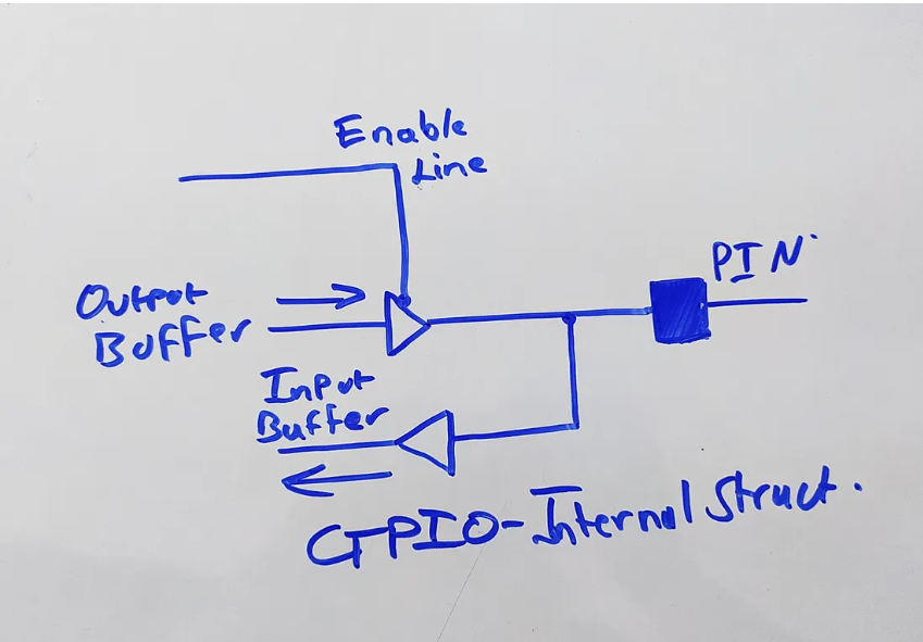
The pins are supported by 2 internal buffers, which are usually D flip-flop shift registers. There is an enable line that controls the direction of movement of the data from these shift registers. When a logical 0 is written at the enable line, the pin is in the OUTPUT mode, and vice versa. In input mode, data is sampled from the pin and stored in the input buffer, and when in output mode, the data stored in the output buffer is shifted bit by bit into the pin, which is then sent to various output devices.
Let’s understand a bit about the 2 types of MOSFETs before we dive into the pin modes.
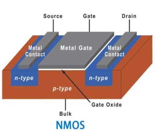
NMOS
NMOS, or N-type Metal Oxide Semiconductor, is a type of MOSFET (Metal Oxide Semiconductor Field Effect Transistor) where the majority carriers are electrons. The name derives from the use of n-type semiconductors as the source and drain regions. Generally, an NMOS transistor is simply built with a p-type body by two n-type semiconductor regions which are adjacent to the gate known as the source & the drain. This transistor has a controlling gate that controls the electron flow between the source & drain terminals.
In this transistor, since the body of the transistor is grounded, the PN junctions of the source & drain toward the body are reverse-biased. If the voltage at the gate terminal is increased, an electric field will start to increase and attracts free electrons to the base of the Si-SiO2 interface.
Once the voltage is high enough, then electrons wind up filling all the holes & a thin region below the gate known as the channel will get inverted to perform as an n-type semiconductor. This will create a conducting lane from the source terminal to the drain by allowing the flow of current, so the transistor will be turned ON. If the gate terminal is grounded then no current flows in the reverse-biased junction so the transistor will be turned OFF.
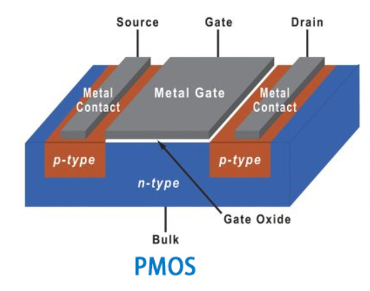
PMOS
PMOS, or P-type Metal Oxide Semiconductor, is another type of MOSFET (Metal Oxide Semiconductor Field Effect Transistor) where the majority carriers are holes. The name comes from the use of p-type semiconductors as the source and drain regions. A pMOS transistor is built with an n-type body including two p-type semiconductor regions which are adjacent to the gate. This transistor has a controlling gate as shown in the diagram which controls the electrons flow between the two terminals like source & drain. In the pMOS transistor, the body is held at +ve voltage. Once the gate terminal is positive, then the source & drain terminals are reverse-biased. Once this happens, there is no flow of current, so the transistor will be turned OFF.
Once the voltage supply at the gate terminal is lowered, then positive charge carriers will be attracted to the bottom of the Si-SiO2 interface. Whenever the voltage gets low sufficiently then the channel will be inverted and creates a conducting pathway from the source terminal to the drain by allowing the flow of current.
Whenever these transistors deal with digital logic there are usually have two different values only like 1 & 0 (ON and OFF). The transistor’s positive voltage is known as VDD which represents the logic high (1) value within digital circuits. The VDD voltage levels in TTL logic were generally around 5V. At present transistors cannot actually withstand such high voltages because they typically range from 1.5V – 3.3V. The low voltage is frequently known as GND or VSS. So, VSS signifies the logic ‘0’ and it is also set normally to 0V.
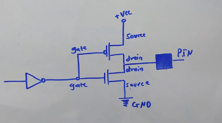
We will see the PMOS being connected to the Positive rail, and the NMOS to the negative rail. This is due to the ability of the NMOS to deliver a strong one and the PMOS to deliver a strong 0!
INPUT MODE
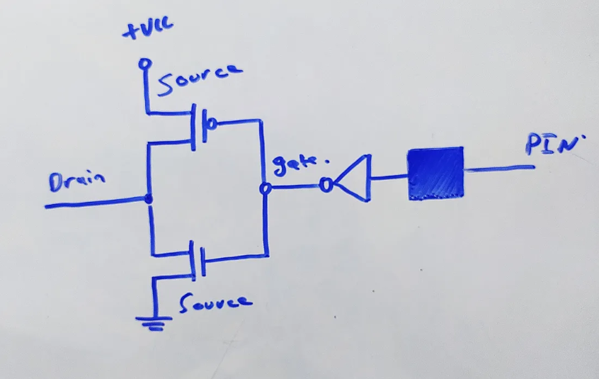
Let’s assume that the pin receives a logic 1 at its input.
- Due to the NOT gate, it is inverted to a 0, which is fed to the PMOS and NMOS transistor circuit.
- This turns on the PMOS Transistor and turns off the NMOS Transistor. As the PMOS is connected to the VCC, it drives the drain terminal to VCC, thus, reading a logic 1 at the input buffer.
If a logic 0 is input at the pin -
- The NOT gate converts it to a logic 1 signal, that is fed to the transistor circuit.
- This turns the NMOS Transistor on and switches the PMOS Transistor off. As the NMOS is connected to the Ground, it drives the drain voltage to GND, thus, reading a logic 0 at the data buffer.
OUTPUT MODE
The output pin configuration is simply a rotation of the input config.
To Write a logic 1 at the output -
- Logic 1 is converted to logic 0 by the NOT gate at the gate of our transistor circuitry.
- When fed to the transistor gates, it turns the PMOS Transistor on and switches the NMOS Transistor off. As the PMOS is connected to the VCC, it drives the output voltage at the pin to the VCC, thus, writing a logic 1 at the output.
To write a Logic 0 at the output -
- Logic 0 is converted to logic 1 by the NOT gate at the gate of our transistor circuitry.
- When fed to the transistor gates, it turns the NMOS Transistor on and switches the PMOS Transistor off. As the NMOS is connected to the Ground, it drives the output voltage at the pin to the GND, thus, writing a logic 0 at the output.
ANALOG INPUT MODE
This is a scam tbh. Because this is not a “MODE” for a GPIO per say, this is simply a channel of an ADC that is mapped to the pin. LOL.
SENSOR & CIRCUIT INTERFACING WITH BASIC GPIOs
Let’s take a look at a couple sensors that we can interact with via using nothing but the basic GPIO pins. We’ll take a look at an IR sensor, and a 7-segment display.
IR SENSORS
Infrared sensors are one of the most common entry points into real-world interfacing. They look deceptively simple, but underneath that tiny blue PCB sits a complete optical detection system. Most commonly, the IR modules you’ll encounter in labs and robotics kits consist of an IR LED that continuously emits infrared radiation, and a photodiode or phototransistor that detects reflected IR light. Alongside this sits a comparator circuit - usually something like an LM358 - which performs the decision-making for you.
Now here’s where things get interesting.
The IR LED emits radiation that is invisible to the human eye but very much alive in the infrared spectrum. When an object comes within range, the emitted IR light reflects off its surface and returns toward the receiver. The photodiode senses this reflected radiation and converts it into a small current. That current is weak and noisy, so the comparator steps in. It compares the sensed signal against a predefined threshold voltage, often adjustable via a potentiometer on the module.
If the reflected signal crosses that threshold, the comparator flips its output state. And that output? It is digital.
This means that from the microcontroller’s perspective, the complexity of analog signal detection has already been handled. The GPIO pin simply reads a HIGH or LOW. There is no need for ADC. There is no need for signal conditioning. The external module has already converted the real-world analog phenomenon of light reflection into a clean digital logic level.
When the GPIO is configured in input mode, it samples the voltage present at the pin. If the comparator drives the line to VCC, the MCU reads a logical 1. If it pulls it to ground, the MCU reads a logical 0. The processor does not know about infrared waves. It does not know about photons. It only knows voltage levels.
And that is the elegance of digital abstraction.
7-Segment Display
Unlike the IR sensor, the 7-segment display is purely an output device. It does not sense. It does not decide. It obeys.
A 7-segment display is nothing more than seven individual LEDs arranged in a figure-eight pattern, optionally with an eighth LED for the decimal point. Each segment is independently controllable. Electrically, each segment behaves exactly like a diode: it emits light when forward biased and remains dark when reverse biased.
There are two common configurations: common anode and common cathode. In the common cathode configuration, all the cathodes of the LEDs are tied together and connected to ground. To illuminate a segment, the corresponding anode must be driven HIGH. In the common anode configuration, all the anodes are tied to VCC, and a segment is illuminated when its cathode is driven LOW.
Now think about what this means in terms of GPIO.
Each segment is connected to a separate GPIO pin. When you want to display a digit, you manually write a pattern of HIGHs and LOWs across those pins. For example, to display the digit “0”, you energize segments a, b, c, d, e, and f, and leave segment g off. The microcontroller does not understand what “0” means. It only outputs a specific binary pattern.
In other words, you are encoding numerical symbols into voltage levels.
The responsibility of current limiting lies entirely on you. Each segment draws current, and each GPIO pin has a maximum sourcing and sinking capability. Exceed those limits, and you damage the pin. The display has no intelligence, no protection logic, and no decoder unless you explicitly add one.
What you are witnessing here is raw digital control. The GPIO output buffer drives a PMOS/NMOS pair that either connects the segment to VCC or to ground. That transistor switching action results in current flow. Current flow results in photon emission. Photon emission results in a glowing segment.
Leave a Comment